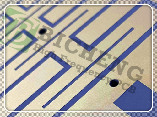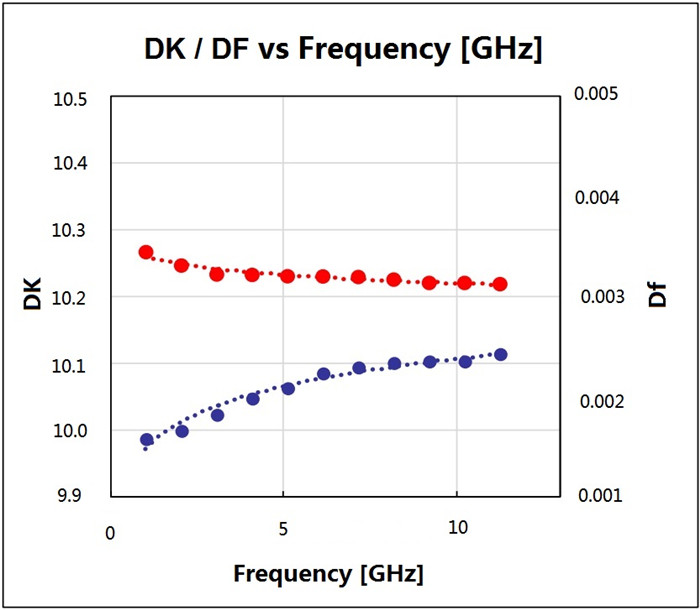
RF-10 2-Layer 0.6mm PCB – 20mil Ceramic-Filled PTFE with Immersion Silver for High-Frequency RF Applications1. Introduction to RF-10 2-Layer 0.6mm PCB RF-10 copper clad laminates are composites of ceramic-filled PTFE and woven fiberglass, offering the advantage of high dielectric constant and low dissipation factor. The thin woven fiberglass reinforcement provides both low dielectric loss and improved rigidity for ease of handling, while enhancing dimensional stability for multilayer circuits. These laminates are engineered to deliver a cost-effective substrate with industry-acceptable delivery times, addressing the need for size reduction in RF applications. RF-10 bonds effectively with smooth low-profile copper, and its low dissipation factor combined with very smooth copper results in optimal insertion losses at higher frequencies where skin effect losses play a substantial role. 2. Key Features Dielectric Constant: 10.2 ± 0.3 at 10GHz 3. Benefits High DK enables RF circuit size reduction
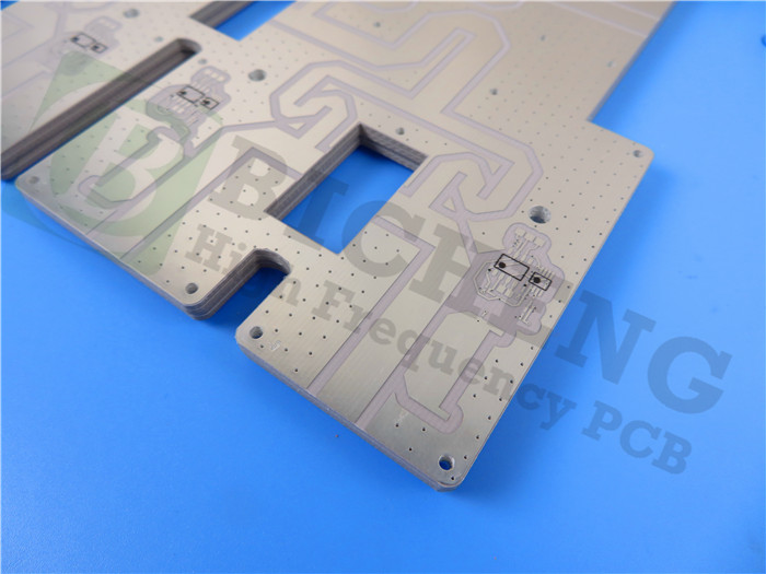
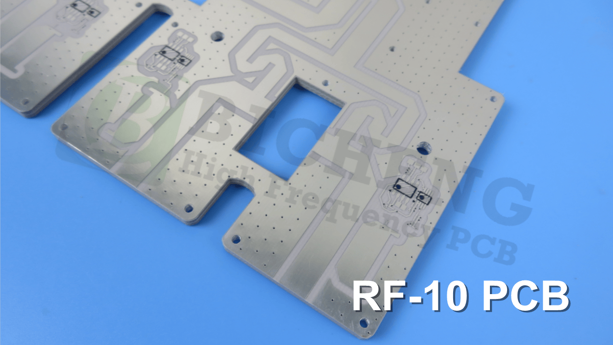
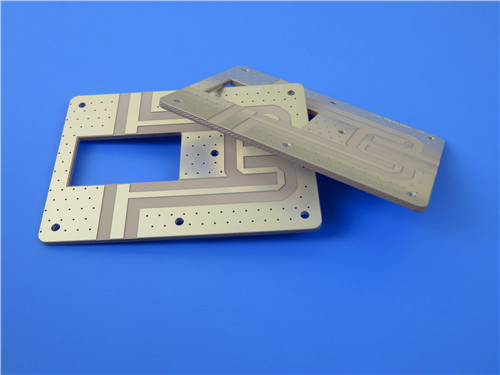
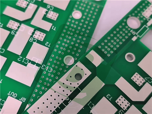
4. PCB Construction Details
5. PCB Stackup (2-Layer Rigid Structure) Copper_layer_1 - 35μm (1oz) 6. PCB Statistics: Components: 19 7. Typical Applications Microstrip patch antennas 8. Quality Assurance Artwork Format: Gerber RS-274-X |
Get a Quick Quote
Fill in the form below and our engineers will reply within 24 hours with technical specifications and pricing for RF-10 2-Layer 0.6mm PCB – 20mil Ceramic-Filled PTFE with Immersion Silver for High-Frequency RF Applications.